
PCB FABRICATION
HDI PCB Manufacturing & Microvia Design Review
VOLUXIN · PCB FABRICATION
Review high-density interconnect requirements using the actual board layout, microvia structure and approved fabrication stack-up.
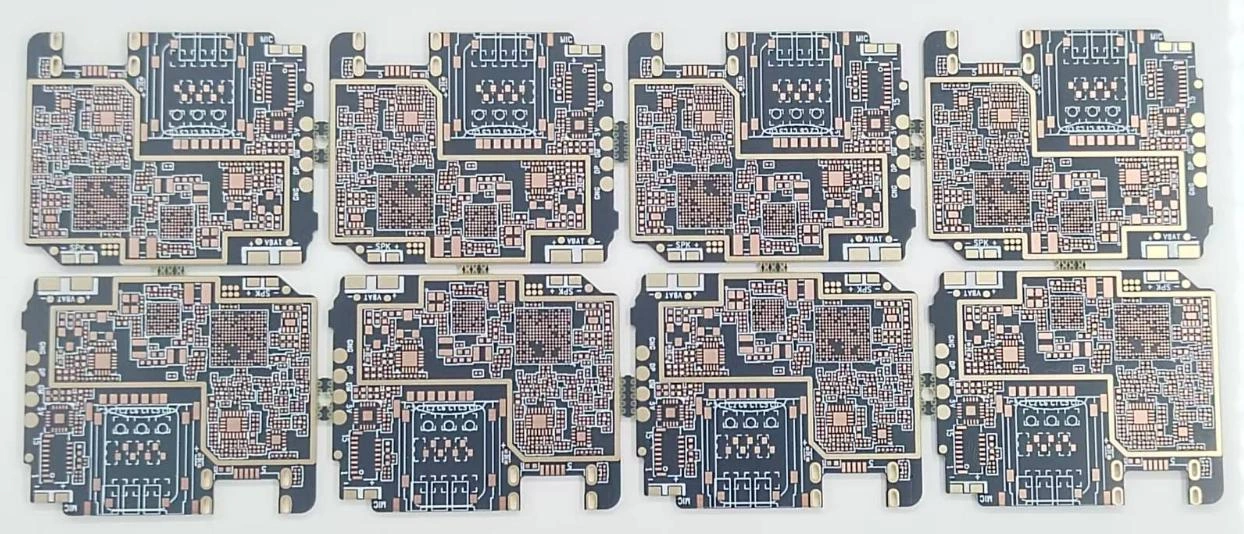
What is an HDI PCB?
A high-density interconnect PCB uses structures such as microvias and build-up layers to support dense routing. The appropriate construction depends on component pitch, connection strategy, reliability requirements and manufacturing constraints.
Plan the HDI fabrication stack-up
| Requirement | What to specify |
|---|---|
| Build-up structure | Define the core, sequential build-up stages and target finished thickness. |
| Microvias | Specify laser-drilled microvia locations, dimensions and connection structure. |
| Via filling | Identify via-in-pad, filled and capped vias, where needed by the design. |
| Routing | Provide required trace widths, spacing and fine-pitch breakout geometry. |
| Verification | Agree electrical test, microsection review and applicable acceptance requirements. |
Compact control and sensing electronics
HDI may be relevant to compact battery-monitoring, communication and control boards when component density creates routing constraints. It is not automatically the best choice for every BMS or power-conversion design. Compare routing needs, manufacturability and cost with a multilayer through-hole construction.
Microsection review
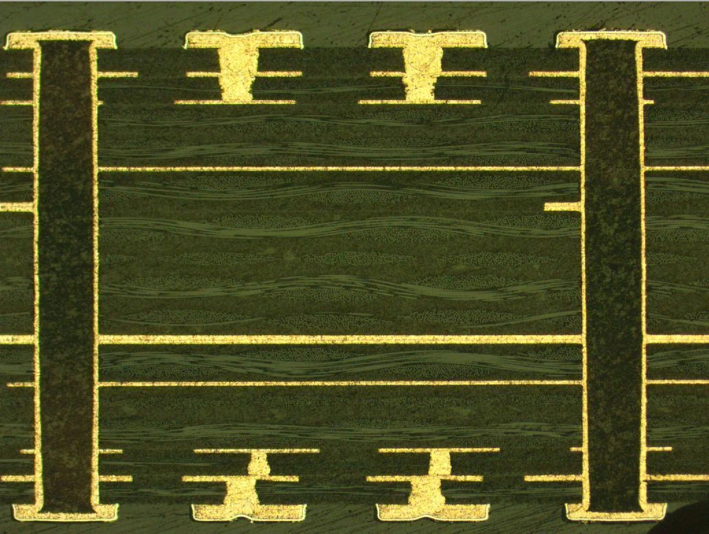
Cross-section review can support agreed checks of interconnections and layer construction. Define the sample method, acceptance criteria and documentation required in the quotation.
HDI PCB manufacturing reference
| Manufacturing item | 2026 reference | Project approval |
|---|---|---|
| Layers and build-up | Up to 14 layers; 1–3 build-up stages | Review the via structure and sequential lamination together. |
| Finished thickness | 0.3–2.4 mm | Approve stack-up and dimensional tolerance. |
| Trace / space | Inner and outer: 2/2 mil | Fine geometry must be reviewed with copper and the actual layout. |
| Through-hole drilling | Minimum through-hole drill bit: 0.15 mm | Separate laser microvia requirements from mechanically drilled holes. |
| Blind-via structure | Microvia and via-in-pad structures require a defined build | Specify filled/capped features and the required verification scope. |
| Verification | Electrical, optical, impedance and microsection review where applicable | Agree sampling, acceptance criteria and report deliverables before ordering. |
Manufacturing reference: 2026 fabrication data, pages 24–25. These entries describe separate process limits, not a guarantee that every limit can be combined in one board. The approved design and quotation define the supplied scope. Future capability plans and the source’s ambiguous BGA-pitch units are excluded.
HDI versus through-hole multilayer PCB
Choose HDI when routing density and component escape requirements justify microvias and sequential build-up. Use a through-hole multilayer construction when it can meet routing, connection and packaging requirements with a simpler fabrication flow. The decision should start with the actual design rather than a target layer count or a marketing label.
For a compact BMS or industrial communication board, provide the pad geometry, via structure and net classes before requesting a build. For power circuitry, treat copper distribution, insulation distances and heat removal as separate design requirements. Microvia density is not a measure of power-handling capability.
Before a sample order, agree filled/capped-via details, the build sequence and what the microsection or other inspection record must establish. Keep the approved fabrication revision attached to repeat enquiries.
Compare multilayer PCB fabrication · Prepare a custom PCB brief · AGV and AMR electronics context
PCB manufacturing questions
Does PCB fabrication include components and assembly?
These pages cover bare printed circuit board fabrication. Component sourcing, SMT assembly, firmware and finished-device testing require a separate scope review; they are not included in a bare-board quotation.
How do I request a PCB manufacturing quote?
Start with board type, layer count, dimensions, quantity and schedule. Add material, copper weight, finished thickness, surface finish and impedance requirements if known. Arrange design-file exchange with VOLUXIN before sending proprietary files.
Is HDI required for every compact BMS board?
No. Routing density, component pitch, interconnection reliability and cost determine whether HDI is appropriate. Compare the proposed HDI structure with a conventional multilayer stack-up during design review.
Discuss your custom PCB project
Share the board type, quantity and fabrication requirements. Start with non-confidential information; agree document exchange before sending design files.
Request a PCB Manufacturing Quote Review fabrication requirements →