
PCB FABRICATION
Multilayer PCB Manufacturing for Power & Control
VOLUXIN · PCB FABRICATION
Prepare a manufacturable stack-up for rigid multilayer boards, with clear material, copper and interconnection requirements.
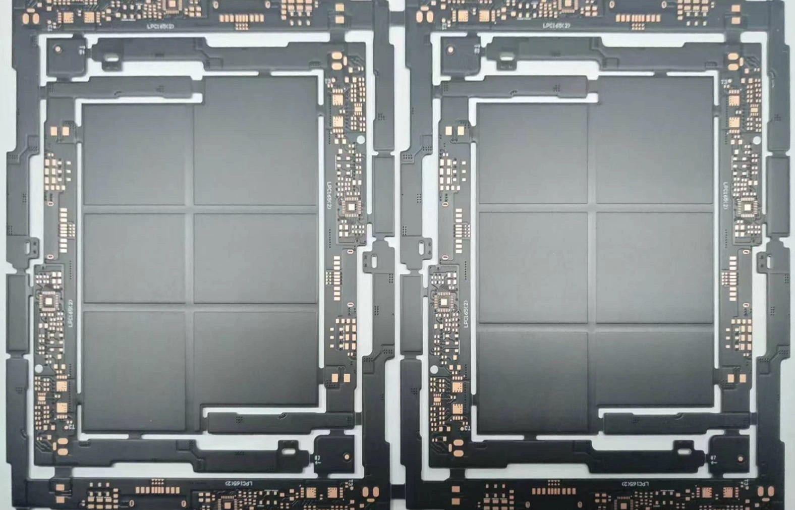
What is a multilayer PCB?
A multilayer PCB combines several patterned copper layers with insulating dielectric layers. Internal planes and signal routing can help organize power distribution and control circuitry. Layer count alone does not determine current capacity, isolation or thermal performance.
Specify a multilayer board
| Requirement | What to specify |
|---|---|
| Stack-up and layers | Proposed layer count, signal and plane assignments, dielectric spacing and total thickness. |
| Material | Requested FR-4 grade or another specified laminate, with temperature and electrical requirements. |
| Copper | Starting and finished copper requirements by layer; state relevant tolerances. |
| Holes and finish | Plated and non-plated holes, finished hole sizes, surface finish and solder mask. |
| Impedance and testing | Controlled-impedance nets, target values and tolerances, electrical test and inspection requirements. |
Power electronics and industrial-control use cases
For BMS control boards, review sensing routes, connector locations and isolation requirements. For DC-DC boards, discuss power-current paths, creepage, clearance and heat dissipation with the circuit designer. For industrial interfaces, define mounting holes, connector keep-outs and the intended operating environment.
DFM questions before placing an order
Check annular rings, drill-to-copper spacing, copper balance, panel layout and fabrication tolerances. Share an approved stack-up rather than relying on an assumed standard build. Available layer counts, copper weights and materials are confirmed for the specific design.
Multilayer PCB fabrication reference
| Manufacturing item | 2026 reference | Project approval |
|---|---|---|
| Layer construction | Through-hole multilayer: up to 28 layers | Approve the material and stack-up for the actual build. |
| Finished thickness | Through-hole: 0.5–4.5 mm | Agree thickness and tolerance with the fabrication drawing. |
| Copper | Through-hole: 1/3–6 oz | Specify starting/finished copper by layer; limits are not simultaneous guarantees. |
| Trace / space | Through-hole inner: 2/2 mil; outer: 2.3/2.3 mil | Review geometry, copper thickness and clearance together. |
| Drilling | Through-hole minimum drill bit: 8 mil | Tool size is not the finished plated-hole diameter. |
| Materials | FR-4 entries include mid/high Tg, high-CTI and halogen-free options | Approve the exact laminate grade; do not substitute by Tg alone. |
| Surface finish | OSP, immersion gold, lead-free HASL, gold-finger and carbon-ink entries | Select a process and agree finish thickness and acceptance criteria. |
Manufacturing reference: 2026 fabrication data, pages 24–25. These entries describe separate process limits, not a guarantee that every limit can be combined in one board. The approved design and quotation define the supplied scope. Future capability plans and the source’s ambiguous BGA-pitch units are excluded.
Choosing a stack-up for BMS and DC-DC boards
Start with the circuit designer’s net classes and current paths. A BMS sensing board needs defined measurement routing and connector clearances; a DC-DC power board needs copper distribution and thermal paths appropriate to its design. Added layers can make routing easier, but layer count and copper weight alone cannot establish circuit performance.
During fabrication review, identify planes, copper balance, dielectric spacing, plated-hole geometry and board flatness requirements. Record the final material grade and approved stack-up as part of the fabrication revision. This makes a repeat order reproducible without relying on an informal board description.
BMS configuration requirements · DC-DC source and load requirements · When to review an HDI construction
PCB manufacturing questions
Does PCB fabrication include components and assembly?
These pages cover bare printed circuit board fabrication. Component sourcing, SMT assembly, firmware and finished-device testing require a separate scope review; they are not included in a bare-board quotation.
How do I request a PCB manufacturing quote?
Start with board type, layer count, dimensions, quantity and schedule. Add material, copper weight, finished thickness, surface finish and impedance requirements if known. Arrange design-file exchange with VOLUXIN before sending proprietary files.
Discuss your custom PCB project
Share the board type, quantity and fabrication requirements. Start with non-confidential information; agree document exchange before sending design files.
Request a PCB Manufacturing Quote Review fabrication requirements →