
PCB FABRICATION
PCB Fabrication Capabilities & Quality Review
VOLUXIN · PCB FABRICATION
A practical framework for agreeing manufacturing scope, inspection requirements and project documentation.
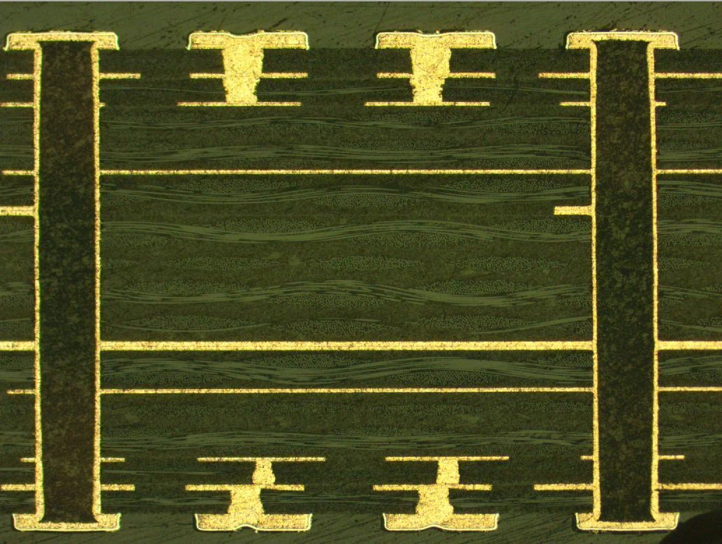
Fabrication processes to discuss
Project reviews can cover imaging, multilayer lamination, mechanical and laser drilling, plating, solder mask, surface finish and board profiling. The required process sequence is determined by the approved design and quotation.
Quality requirements belong in the specification
| Requirement | What to specify |
|---|---|
| Optical inspection | Agree AOI or final visual inspection scope and defect acceptance criteria. |
| Electrical testing | Define the bare-board connectivity and isolation test requirements. |
| Controlled impedance | Provide target values, tolerances and any coupon or report requirements. |
| Microsection | Agree sampling and the features to be examined. |
| Documentation | Request the applicable inspection records and current qualification documents before order approval. |
DFM inputs and file preparation
Prepare Gerber or another agreed data format, drill files, fabrication notes, stack-up, dimensions and panel instructions. Clearly identify plated holes, slots, controlled impedance and special materials. BOM and placement data are assembly inputs and are not mandatory for a bare-board fabrication enquiry.
Confirm current capability for your design
Maximum layer count, minimum trace spacing, material availability, copper weight, tolerances and lead time depend on the proposed build. Request written confirmation for your design. Qualification documents must match the manufacturing scope and issuing entity; application descriptions are not certification claims.
PCB fabrication capability matrix
| Process item | 2026 reference | Project approval |
|---|---|---|
| Layer construction | Through-hole multilayer: up to 28 layers | Approve the material and stack-up for the actual build. |
| Finished thickness | Through-hole: 0.5–4.5 mm | Agree thickness and tolerance with the fabrication drawing. |
| Copper | Through-hole: 1/3–6 oz | Specify starting/finished copper by layer; limits are not simultaneous guarantees. |
| Trace / space | Through-hole inner: 2/2 mil; outer: 2.3/2.3 mil | Review geometry, copper thickness and clearance together. |
| Drilling | Through-hole minimum drill bit: 8 mil | Tool size is not the finished plated-hole diameter. |
| Layers and build-up | Up to 14 layers; 1–3 build-up stages | Review the via structure and sequential lamination together. |
| Finished thickness | 0.3–2.4 mm | Approve stack-up and dimensional tolerance. |
| Trace / space | Inner and outer: 2/2 mil | Fine geometry must be reviewed with copper and the actual layout. |
| Through-hole drilling | Minimum through-hole drill bit: 0.15 mm | Separate laser microvia requirements from mechanically drilled holes. |
Manufacturing reference: 2026 fabrication data, pages 24–25. These entries describe separate process limits, not a guarantee that every limit can be combined in one board. The approved design and quotation define the supplied scope. Future capability plans and the source’s ambiguous BGA-pitch units are excluded.
Inspection scope and evidence to request
| Review | Purpose | Record to agree |
|---|---|---|
| Optical inspection | Copper features or finished-board appearance | Inspection stage, criteria, sampling and report scope. |
| Bare-board electrical test | Connectivity and isolation of the unpopulated board | Net data, test method and agreed acceptance requirement. |
| Impedance review | Specified nets or agreed test coupon | Target, tolerance, construction, measurement and record. |
| Microsection | Defined interconnection or stack-up features | Sample location, features measured and acceptance criteria. |
A blank checklist is not a completed test report. Ask for evidence tied to your board revision and manufacturing scope. Bare-board testing does not replace assembled-circuit or system validation.
From files to a reproducible production order
- Identify one fabrication revision and provide a complete file manifest.
- Resolve DFM questions, material choice, stack-up, holes, panel and finish.
- Approve the manufacturing drawing and the quoted inspection scope.
- Agree sample acceptance, open-issue handling and repeat-order change control.
Review engineering evidence and document scope · Multilayer process requirements · HDI structure requirements
PCB manufacturing questions
Does PCB fabrication include components and assembly?
These pages cover bare printed circuit board fabrication. Component sourcing, SMT assembly, firmware and finished-device testing require a separate scope review; they are not included in a bare-board quotation.
How do I request a PCB manufacturing quote?
Start with board type, layer count, dimensions, quantity and schedule. Add material, copper weight, finished thickness, surface finish and impedance requirements if known. Arrange design-file exchange with VOLUXIN before sending proprietary files.
Discuss your custom PCB project
Share the board type, quantity and fabrication requirements. Start with non-confidential information; agree document exchange before sending design files.
Request a PCB Manufacturing Quote Review fabrication requirements →
VOLUXIN · CUSTOM PROJECT REVIEW
Custom PCB fabrication: match your design to the manufacturing route
Use the 2026 fabrication reference to prepare a multilayer PCB or HDI PCB enquiry. The limits below are manufacturing-reference entries for design review, not a promise that all limits can be combined on one board.
On small screens, scroll the table horizontally to view every review item.
| Review area | Catalogue-backed starting point | Your customisation input |
|---|---|---|
| Through-hole multilayer | Up to 28 layers; finished thickness 0.5–4.5 mm; copper entries 1/3–6 oz. | Submit layer sequence, laminate requirements and copper distribution for a stack-up review. |
| HDI construction | Up to 14 layers; 1–3 build-up stages; finished thickness 0.3–2.4 mm. | Provide the via structure and build-up sequence; quote against the approved fabrication revision. |
| Geometry and drilling | Through-hole reference: inner 2/2 mil and outer 2.3/2.3 mil trace/space; minimum drill bit 8 mil. | State finished plated-hole dimensions and tolerances separately from drill-bit sizes. |
| Materials, finish and inspection | FR-4 material categories and OSP, immersion-gold, lead-free HASL and gold-finger finish entries are documented. | Specify the exact material and finish; agree electrical test, impedance and microsection records as applicable. |
Only the 2026 reference is used. Later capability and capacity plans are excluded. Ambiguous source units are not used as design limits.