
PCB FABRICATION
Custom PCB Manufacturing | Multilayer & HDI PCB
VOLUXIN · BARE PRINTED CIRCUIT BOARD FABRICATION
Custom PCB manufacturing for OEM electronics starts with a clear board specification. VOLUXIN handles multilayer PCB and HDI PCB fabrication enquiries for battery management, DC-DC power conversion and industrial-control projects, from prototype requirements to repeat-production planning.
Get a PCB fabrication review
Tell us your board type, layer count, dimensions and quantity. We will review the manufacturing requirements and confirm the proposed scope, documentation and quotation details.
What is PCB manufacturing?
Printed circuit board manufacturing, also called PCB fabrication, turns approved design data into a bare circuit board. The board contains the copper interconnections, insulating layers, drilled features and protective finishes specified by the design. Components are added during a separate PCB assembly stage.
This page helps engineering and purchasing teams define a custom board order. Use the manufacturing checklist to compare suppliers on the same stack-up, materials, tolerances and inspection scope.
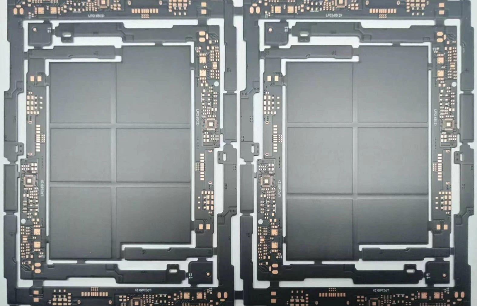
Multilayer PCB manufacturing and HDI PCB fabrication
Multilayer PCB manufacturer enquiries
Discuss rigid multilayer printed circuit boards for power distribution, control signals and industrial interfaces. Specify the copper layers, dielectric spacing, plated-through-hole construction and total board thickness.
HDI PCB manufacturing enquiries
High-density interconnect boards use structures such as microvias and build-up layers to address dense routing. Share the component pitch, via structure and stack-up for a design-specific feasibility review.
| Design question | Multilayer through-hole construction | HDI construction |
|---|---|---|
| Routing and interconnections | Review internal planes, signal layers and through-hole routes. | Review fine-pitch breakout, microvias and build-up layers. |
| Manufacturing inputs | Define stack-up, copper, drilled holes and board geometry. | Also define microvia connections, via filling and lamination sequence. |
| Selection trade-off | Compare routing space, materials and fabrication cost. | Compare density benefits against added process complexity and validation needs. |
Available layer counts and feature limits are confirmed for your design. A PCB example is not a universal manufacturing limit or a guarantee that another design can use the same process.
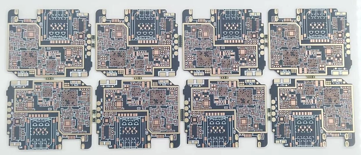
Custom PCBs for BMS, DC-DC converters and industrial electronics
Application-specific PCB fabrication begins with the circuit designer’s requirements. The examples below explain what to review; they do not establish finished-system compatibility or industry certification.
| Application / board | Manufacturing requirements to discuss | Continue the project review |
|---|---|---|
| BMS PCB manufacturing | Battery-sensing connections, isolation boundaries, connector locations, board geometry and fabrication tolerances. | Battery management systems |
| PCB fabrication for DC-DC converters | Power-current routes, copper requirements, creepage and clearance, mounting and thermal constraints. | DC-DC modules and converters |
| AGV and AMR controller PCBs | Control interfaces, communication connectors, routing density and enclosure dimensions. | AGV and AMR applications |
| Forklift and warehouse-equipment interface boards | Connector keep-outs, mounting holes, environmental requirements and inspection scope. | Material-handling applications |
| Industrial-control PCB fabrication | Signal and power separation, controlled-impedance needs, stack-up and panel instructions. | Industrial electrification |
| Battery-powered cleaning-machine electronics | Board dimensions, control connections, mechanical fit and intended operating conditions. | Floor-cleaning applications |
Prototype PCB fabrication to repeat-production planning
Prototype PCB manufacturing helps a team evaluate its proposed construction before committing to a repeat order. Low-volume PCB production and production quantities should use an agreed drawing revision, stack-up and inspection plan.
- Prototype brief: identify the design revision, evaluation quantity and open fabrication questions.
- Sample review: agree the required manufacturing records and let your engineering team validate mechanical fit and circuit performance.
- Production release: freeze approved fabrication data and document any material substitutions or tolerance changes.
- Repeat orders: reference the approved revision and confirm whether the quantity, schedule or inspection scope has changed.
Send your target schedule early. Sample availability, minimum order quantity and delivery terms are confirmed for each quotation.
PCB manufacturing quote checklist: what to send
A complete PCB specification reduces assumptions during quotation. If a value is undecided, mark it for review rather than accepting an unspecified default.
| Quote input | Information to provide |
|---|---|
| Board type and revision | Rigid multilayer or HDI, drawing number and revision; state the intended use. |
| Dimensions and thickness | Finished outline, dimensions, slots, mounting holes, thickness and tolerances. |
| Layer count and stack-up | Layer sequence, dielectric spacing, copper distribution and plane assignments. |
| Laminate / FR-4 material | Requested laminate grade and relevant thermal or electrical requirements. |
| Copper weight | Starting or finished copper requirements by layer; distinguish them clearly. |
| Holes and vias | Plated and non-plated holes, finished sizes, microvia structure, filling and capping where needed. |
| Surface finish and solder mask | Requested finish, mask requirements, exposed pads and any contact-finger details. |
| Controlled impedance | Target values, tolerances, referenced layers, coupons and required records. |
| Panel and inspection | Panel layout, tooling features, electrical test, optical inspection and special acceptance notes. |
| Order and schedule | Sample and production quantities, target dates and shipping destination. |
Download the English PCB requirements checklist (CSV) ↓
Start with non-confidential requirements in the PCB quote form. Agree a suitable exchange through info@voluxin.com before sending proprietary fabrication files. This page does not provide public design-file uploads.
PCB manufacturing process: from design data to bare boards
The process route depends on the approved construction. A multilayer through-hole board and an HDI board may require different drilling and lamination sequences.
- Manufacturing-data review: check the file set, outline, drill data, layer mapping and fabrication notes.
- Imaging and copper-pattern formation: prepare the circuit patterns for the specified layers.
- Lamination: combine conductor and dielectric layers according to the approved stack-up; HDI build-up may use sequential stages.
- Drilling and plating: produce the agreed holes and interconnections, using mechanical or laser processes where specified.
- Solder mask, finish and profiling: complete the protective layers, exposed-contact finish and board outline.
- Inspection and shipment review: complete the agreed bare-board tests, records and order documentation.
PCB DFM review: resolve manufacturability questions early
Design for manufacturability (DFM) focuses on whether the proposed PCB features can be produced within the agreed process and tolerances. It is different from circuit simulation, firmware development and finished-product safety validation.
- Check trace spacing, annular rings and drill-to-copper clearances against the proposed build.
- Clarify stack-up, copper balance and the finished board thickness.
- Identify via-in-pad, blind or buried interconnections and any filled or capped features.
- Check panel layout, edge features, tooling holes and assembly keep-outs provided by the designer.
- Resolve contradictory drawings or missing fabrication notes before approving production.
Bare-board quality inspection and documentation
Specify inspection requirements before ordering. Optical inspection examines board features, while electrical testing checks the intended bare-board connectivity and isolation. Controlled-impedance and microsection reviews address different parts of the fabrication specification.
| Review area | Define in your order |
|---|---|
| AOI / visual inspection | Inspection scope and agreed defect acceptance criteria. |
| Bare-board electrical testing | Required test coverage and record format. |
| Controlled impedance | Target values, tolerances, coupons and report requirements. |
| Microsection review | Sampling method, interconnection features and acceptance criteria. |
| Qualification documents | Current documents applicable to the quoted manufacturing scope and issuing entity. |
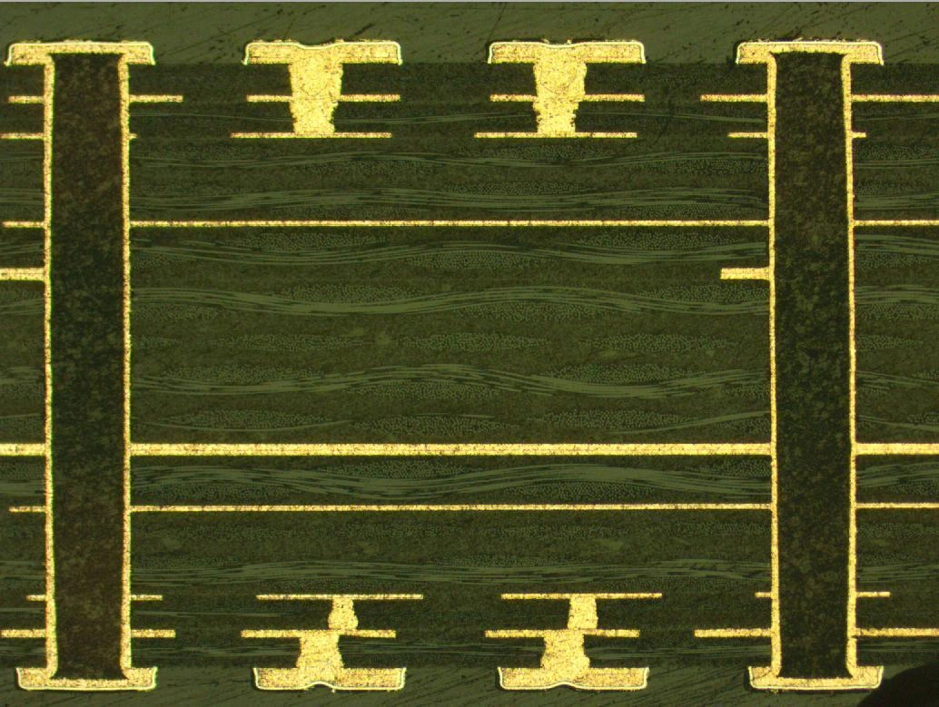
State any required acceptance standard and revision in your fabrication notes. VOLUXIN will review it with the proposed manufacturing scope; a standards reference here is not a certification claim.
What affects PCB manufacturing cost and lead time?
Compare custom PCB quotes using the same technical specification. A lower quoted price may cover a different material, tolerance, test plan or quantity.
- Board area and panel utilization: outline and panel layout influence material use.
- Layer count and stack-up: construction complexity changes the fabrication route.
- Material and copper: laminate availability and copper requirements affect process choices.
- Via structures: microvias, filling and sequential lamination add manufacturing considerations.
- Finish and tolerances: special features require an explicit scope.
- Quantity and inspection: setup, sampling and requested reports influence the quotation.
For quick-turn PCB enquiries, share the deadline and identify which specifications are fixed. Expedite feasibility and any schedule commitment must be confirmed in writing for the proposed build.
PCB manufacturing FAQs
What does a custom PCB manufacturer need for a quote?
For a preliminary review, provide the PCB type, layer count, board dimensions, quantity and target schedule. For a manufacturing quotation, prepare the fabrication data, drill files, stack-up, material, finished thickness, copper requirements, surface finish and inspection notes. Identify any undecided items rather than leaving them implicit.
What is the difference between PCB fabrication and PCB assembly?
PCB fabrication produces the bare board with copper circuits, holes, solder mask and surface finish. PCB assembly adds electronic components and soldering. VOLUXIN’s PCB pages cover bare-board fabrication; component sourcing, SMT assembly, firmware and finished-board functional testing require a separate scope review.
Should I choose a multilayer PCB or an HDI PCB?
Start with routing density and interconnection needs. A conventional multilayer construction may suit many power and control boards. HDI can address compact layouts and fine-pitch routing through microvias and build-up layers. Compare the actual stack-up, reliability requirements, manufacturability and cost before deciding.
Can I request prototype PCBs and low-volume PCB production?
Yes. Send prototype, sample or low-volume fabrication requirements for review. Minimum order quantity, sample quantity, setup costs and production schedule are confirmed in the quotation for the proposed board; no universal minimum or quick-turn delivery time is assumed.
How should I specify a PCB for a BMS or DC-DC converter?
For a BMS board, identify sensing connections, isolation boundaries, connector layout and mounting constraints. For a DC-DC power board, specify copper requirements, current paths, thermal constraints, creepage and clearance in the design. The circuit designer must verify electrical performance and system safety; bare-board fabrication does not provide that validation.
Can I request FR-4, controlled impedance or heavier copper?
Include the requested FR-4 laminate grade, copper requirements by layer and any controlled-impedance targets in the project brief. State tolerances, relevant test coupons and report requirements. Material availability and the manufacturability of the combined specification must be confirmed before an order is approved.
Which files are needed for PCB fabrication?
Prepare Gerber or another agreed manufacturing format, drill data, an outline drawing, fabrication notes and a stack-up specification. Add panel instructions and an impedance table when relevant. BOM and component-placement files are assembly inputs and are not required for a bare-board enquiry. Arrange document exchange with VOLUXIN before sending proprietary designs.
What affects PCB manufacturing cost and lead time?
Layer count, board area, panel utilization, laminate, copper weight, via structure, surface finish, tolerances, inspection scope and order quantity all affect the quotation. Special materials or additional lamination cycles can change the schedule. Compare quotes using the same approved fabrication specification.
What PCB quality documents should I request?
Agree the bare-board electrical test, optical inspection and any impedance or microsection records required for your project. State the requested acceptance standard and revision in the fabrication notes. Ask for current qualification documents that match the quoted manufacturing scope; this page is not a claim of certification.
Request a custom PCB manufacturing quote
Ready to discuss multilayer PCB fabrication, HDI manufacturing or a PCB for your BMS, DC-DC or industrial-control design? Share your board requirements and quantity with VOLUXIN.
Send PCB Project Requirements Review PCB manufacturing requirements →
VOLUXIN · CUSTOM PROJECT REVIEW
Custom PCB fabrication: match your design to the manufacturing route
Use the 2026 fabrication reference to prepare a multilayer PCB or HDI PCB enquiry. The limits below are manufacturing-reference entries for design review, not a promise that all limits can be combined on one board.
On small screens, scroll the table horizontally to view every review item.
| Review area | Catalogue-backed starting point | Your customisation input |
|---|---|---|
| Through-hole multilayer | Up to 28 layers; finished thickness 0.5–4.5 mm; copper entries 1/3–6 oz. | Submit layer sequence, laminate requirements and copper distribution for a stack-up review. |
| HDI construction | Up to 14 layers; 1–3 build-up stages; finished thickness 0.3–2.4 mm. | Provide the via structure and build-up sequence; quote against the approved fabrication revision. |
| Geometry and drilling | Through-hole reference: inner 2/2 mil and outer 2.3/2.3 mil trace/space; minimum drill bit 8 mil. | State finished plated-hole dimensions and tolerances separately from drill-bit sizes. |
| Materials, finish and inspection | FR-4 material categories and OSP, immersion-gold, lead-free HASL and gold-finger finish entries are documented. | Specify the exact material and finish; agree electrical test, impedance and microsection records as applicable. |
Only the 2026 reference is used. Later capability and capacity plans are excluded. Ambiguous source units are not used as design limits.